- UCAS course code
- H614
- UCAS institution code
- M20
Overview
- Degree awarded
- MEng
- Duration
- 4 years
- Typical A-level offer
-
AAA including Mathematics and either Physics, Electronics, Further Mathematics, Chemistry or Computer Science.
- Typical contextual A-level offer
-
AAB including Mathematics and either Physics, Electronics, Further Mathematics, Chemistry or Computer Science.Find out more about contextual admissions.
- Refugee/care-experienced offer
-
Applicants who have been in local authority care for more than three months or have refugee status may be eligible for an offer two grades below the standard requirements.Find out more about contextual admissions.
- Typical International Baccalaureate offer
-
36 points overall with 6,6,6 in Higher Level subjects, including 6 in Mathematics, 6 in Physics or Chemistry, and 6 in one other Higher Level subject.
For this programme of study we will accept: Higher Level Mathematics: Analysis and Approaches or Mathematics: Applications and Interpretation
Applicants studying the International Baccalaureate Career Related Programme (IBCP) should contact the academic School prior to applying so that their academic profile can be considered.
- How to apply
Apply through UCAS .
- Sustainable Development Goals
Find out how this course aligns to the UN Sustainable Development Goals, including learning which relates to:
- Goal 7: Affordable and clean energy
- Goal 9: Industry, innovation and infrastructure
- Goal 11: Sustainable cities and communities
- Goal 12: Responsible consumption and production
- Goal 13: Climate action
- UCAS course code
- H614
- UCAS institution code
- M20
Course overview
- Study at one of the largest departments in the country, with a distinguished history & a focus on the future.
- Complete your degree with a final-year team project directly funded by industry or inspired by industrial needs.
- Combine scientific & engineering knowledge with creativity to solve some of today's biggest electronic engineering challenges making use of an incredible array of equipment & facilities.
- Study at a university ranked 4th for electrical & electronic engineering in the UK (QS World University Rankings 2023).
- We're the most targeted university by the UK's leading graduate employers ( High Fliers Research 2023 ).
- Learn in our brand-new, purpose-built space for innovation and creativity. Explore Our Home for Engineering and Materials.
Open days
The University holds undergraduate open days regularly, giving you the opportunity to find out more about our courses, the support we offer, and our facilities. Attending an open day is a great way to find out what studying at Manchester is all about. Find out about our upcoming open days .
Fees
Tuition fees for home students commencing their studies in September 2024 will be £9,250 per annum. Tuition fees for international students will be £32,500 per annum. For general information please see the undergraduate finance pages.
Policy on additional costs
All students should normally be able to complete their programme of study without incurring additional study costs over and above the tuition fee for that programme. Any unavoidable additional compulsory costs totalling more than 1% of the annual home undergraduate fee per annum, regardless of whether the programme in question is undergraduate or postgraduate taught, will be made clear to you at the point of application. Further information can be found in the University's Policy on additional costs incurred by students on undergraduate and postgraduate taught programmes (PDF document, 91KB).
Scholarships/sponsorships
For information about scholarships and bursaries please visit our undergraduate student finance pages and our Department funding pages .
UN Sustainable Development Goals
The 17 United Nations Sustainable Development Goals (SDGs) are the world's call to action on the most pressing challenges facing humanity. At The University of Manchester, we address the SDGs through our research and particularly in partnership with our students.
Led by our innovative research, our teaching ensures that all our graduates are empowered, inspired and equipped to address the key socio-political and environmental challenges facing the world.
To illustrate how our teaching will empower you as a change maker, we've highlighted the key SDGs that our courses address.
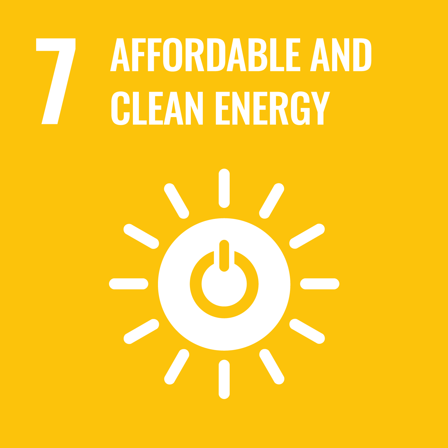
Goal 7: Affordable and clean energy
Ensure access to affordable, reliable, sustainable and modern energy for all

Goal 9: Industry, innovation and infrastructure
Build resilient infrastructure, promote inclusive and sustainable industrialization and foster innovation
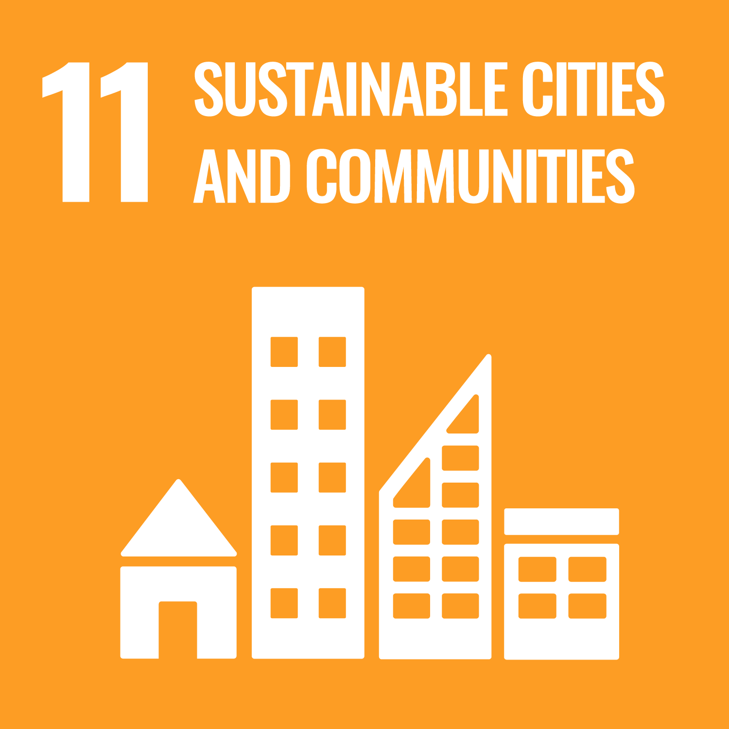
Goal 11: Sustainable cities and communities
Make cities and human settlements inclusive, safe, resilient and sustainable
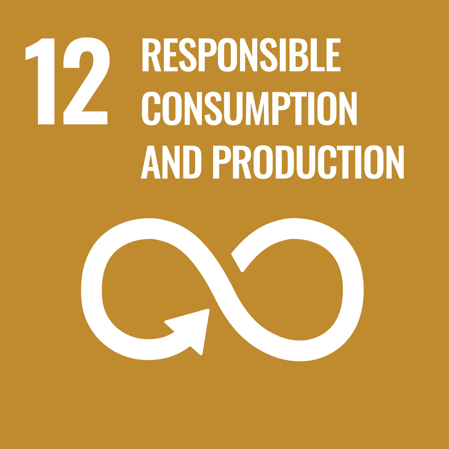
Goal 12: Responsible consumption and production
Ensure sustainable consumption and production patterns

Goal 13: Climate action
Take urgent action to combat climate change and its impacts
Contact details
- Department
- Department of Electrical & Electronic Engineering
- Contact name
- Undergraduate Admissions team
- Telephone
- +44 (0)161 275 4300
- ug-eee@manchester.ac.uk
- Website
- https://www.eee.manchester.ac.uk/
- School/Faculty overview
-
The School of Engineering creates a world of possibilities for students pursuing skills and understanding. Through dynamic research and teaching we develop engineering solutions that make a difference to society in an ethical and sustainable way. Science-based engineering is at the heart of what we do, and through collaboration we support the engineers and scientists of tomorrow to become technically strong, analytically innovative and creative. Find out more about Science and Engineering at Manchester .
Courses in related subject areas
Use the links below to view lists of courses in related subject areas.
Compare this course
Entry requirements
A-level
AAA including Mathematics and either Physics, Electronics, Further Mathematics, Computer Science or Chemistry.
If you do not have the required grades or subjects you may want to consider our integrated foundation year.
Practical skills are a crucial part of science education and therefore there will be a requirement to pass the practical element of any science A Level taken. Where applicants are applying for science and related degrees, this is likely to be made explicit in the offers you will receive.
Contextual offer
AAB including Mathematics and either Physics, Electronics, Further Mathematics, Chemistry or Computer Science.
Practical skills are a crucial part of science education and therefore there will be a requirement to pass the practical element of any science A Level taken. Where applicants are applying for science and related degrees, this is likely to be made explicit in the offers you will receive.
Duration of A-level study
Your application will be considered against the standard selection process of your chosen course if you either:
a) sat your examinations early;
or
b) followed an accelerated curriculum and spent three years studying A-levels where the examinations were taken over two years.
If you are studying an advanced curriculum where the examinations are spread over three years, consideration for an offer will be at the discretion of the admissions tutor for that subject.
AS-level
Unit grade information
The University of Manchester welcomes the provision of unit information where available. Like all other information provided by applicants this may be taken into consideration when assessing your application. Unit grades will not normally form part of an offer conditions.
GCSE
Applicants must demonstrate a broad general education, typically five GCSEs/iGCSEs, including acceptable levels of literacy and numeracy, equivalent to at least Grade B/6 in GCSE/iGCSE English Language and Grade C/5 in GCSE/iGCSE Mathematics.
GCSE/iGCSE English Literature will not be accepted in lieu of GCSE/iGCSE English Language.
Students eligible for a contextual offer will be required to evidence English language proficiency at GCSE English Language grade C/5.
International Baccalaureate
36 points overall with 6,6,6 in Higher Level subjects, including 6 in Mathematics, 6 in Physics or Chemistry, and 6 in one other Higher Level subject.
For this programme of study we will accept: Higher Level Mathematics: Analysis and Approaches or Mathematics: Applications and Interpretation
Applicants studying the International Baccalaureate Career Related Programme (IBCP) should contact the academic School prior to applying so that their academic profile can be considered.
Other international entry requirements
We accept a range of qualifications from different countries. For courses in the Department of Electrical and Electronic Engineering see the accepted entry qualifications from your country .
Scottish requirements
We require grades AAABB in Scottish Highers, including Mathematics and either Physics or Chemistry. In addition, Scottish Advanced Highers are required in one of the following combinations:
Two Advanced Highers AA (including Advanced Highers Mathematics and either Physics, Chemistry or Mathematics of Mechanics), plus two Highers with AA in two different academic subjects (these can be achieved in a previous sitting).
or
Three Advanced Highers AAA (including Advanced Highers Mathematics and either Physics, Chemistry or Mathematics of Mechanics)
English Language not taken at Higher/Advanced Higher must have been achieved at SCQF level 5 (minimum National 5 grade B / Intermediate 2 grade B / Standard Grade 2).
If you require further clarification about the acceptability of this qualification please contact the Academic Department (s) you plan to apply to.
Welsh Baccalaureate
he University welcomes and recognises the value of the Welsh Baccalaureate Advanced Diploma/Advanced Skills Challenge Certificate and requires two A Levels including Maths and one Science subject to be included within this.
The minimum grade required will normally be the same as the lowest grade listed in the A Level entry requirements.
European Baccalaureate
AQA Baccalaureate
The University recognises the benefits of the AQA Baccalaureate and the opportunities it provides for applicants to develop independent study and research skills.
In making offers, the University will focus on the three A Levels taken within the AQA Baccalaureate. The A-Level requirements for the Department of Electrical and Electronic Engineering are AAA including Mathematics and either Physics, Electronics, Further Mathematics, Computer Science or Chemistry.
The units of broader study, enrichment activities and the Extended Project are considered to be valuable elements of the AQA Baccalaureate and we would therefore strongly encourage students to draw upon these experiences within their personal statement.
Foundation year
Foundation year
Applicants completing the Northern Consortium (NCUK) International Foundation Year or INTO Manchester International Foundation in Science and Engineering are required to achieve A*AA including Mathematics, one of either Physics, Chemistry or Further Mathematics, and a third academic subject. An EAP score of A is required.
An excellent performance in local examinations before starting the NCUK Foundation Year, particularly in mathematics and physical science subjects, is also required. Your qualifications prior to the NCUK Foundation Year will be benchmarked against the entry requirements for The University of Manchester BEng (Hons) Electrical, Electronic and Mechatronic Engineering with an Integrated Foundation Year.
The University also recognises a number of external foundation courses as suitable for entry to this undergraduate programme. Assessment will be made on a case-by-case basis and applicants will be expected to meet the entry requirements for The University of Manchester BEng (Hons) Electrical, Electronic and Mechatronic Engineering with an Integrated Foundation Year in their academic qualifications prior to the foundation course. Applicants studying other foundation programmes should contact the academic department to check if their qualification is recognised for entry to this programme and for specific entry requirements.
Pearson BTEC qualifications
Pearson BTEC Level 3 National Extended Diploma
We consider the National Extended Diploma for entry provided it is in Electrical and Electronic Engineering with grades D*DD including Distinction in Further Engineering Mathematics. This should be in combination with a grade B in A-level Mathematics.
Pearson BTEC Level 3 National Diploma
We consider the National Diploma for entry provided it is in Electrical and Electronic Engineering with Grades D*D, in combination with grade A in A-level Mathematics. If you are studying the general Engineering stream, please contact the admissions office to request a full list of the units we require.
Pearson BTEC Level 3 National Foundation Diploma
We consider the National Foundation Diploma for entry in any subject provided it is in combination with two A-levels. Entry requirements are based on achievement of the full National Foundation Diploma with grade D plus two A-levels at grades AA including A in Mathematics and A in any of the following: Physics, Electronics, Chemistry, Computer Science or Further Mathematics.
Pearson BTEC Level 3 National Extended Certificate
We consider the National Extended Certificate for entry in any subject at D provided it is in combination with two GCE A Levels at grades AA including A in Mathematics and A in any of the following: Physics, Electronics, Chemistry, Computer Science or Further Mathematics.
If you require further clarification about the acceptability of this qualification please contact the academic School(s) you plan to apply to.
OCR Cambridge Technical qualifications
Cambridge Level 3 Technical Extended Diploma (CTEC)
We consider the Cambridge Technical Extended Diploma for entry provided it is in Engineering with grades D*DD, in combination with a grade B in A-level Mathematics.
Cambridge Level 3 Technical Diploma (CTEC)
We consider the Cambridge Technical Diploma for entry provided it is in Engineering with grades DD in combination with a grade A in A level Mathematics.
Cambridge Level 3 Technical Foundation Diploma (CTEC)
We consider the Technical Foundation Diploma for entry with Grades DD, in combination with grade A in A-level Mathematics and Grade A in either Physics, Electronics, Further Mathematics, Computer Science or Chemistry.
Cambridge Level 3 Technical Extended Certificate (CTEC)
We consider the Cambridge Technical Extended Certificate for entry in any subject at grade D provided it is in combination with two A levels at grades AA including A in Mathematics and A in either Physics, Electronics, Further Mathematics, Computer Science or Chemistry.
If you require further clarification about the acceptability of this qualification please contact the academic department(s) you plan to apply to.
Access to HE Diploma
Each application is considered individually. Applicants should contact the Admissions Office to discuss their particular circumstances.
Our standard academic requirements include 60 credits in an engineering related subject, with 45 credits at Level 3 with a Distinction grade. A minimum of 15 credits must be in Mathematics. Students are also required to have a grade A in A-level Mathematics with a pure element.
Cambridge Pre-U
D3 in three Principal subjects, including Mathematics and either Physics, Further Mathematics or Chemistry.
We also consider applicants offering Pre-U Principal Subjects, or a mix of Pre-U and A-level subjects, in three distinct subjects.
The University welcomes and recognises the value of the Cambridge Pre-U Global Perspectives and Research (GPR) and the opportunities it provides for applicants to develop independent study and research skills. However, the qualification will not form part of your offer conditions.
T Level
We do not accept T Levels as entry onto this course. The University does accept specific T Level qualifications on a number of courses please review to our T Level information page for a full list.
Extended Project Qualification (EPQ)
Core Maths
The University welcomes and recognises the value of Level 3 core mathematics qualifications (e.g. AQA Certificate in Mathematical Studies).
Core Mathematics is not a compulsory element of post-16 study and as a result we will not normally include it in the conditions of any offer made to the student. However, if a student chooses to undertake a core mathematics qualification this may be taken into account when we consider their application, particularly for certain non-science courses with a distinct mathematical or statistical element.
We advise students to contact the academic Department, who will clarify whether their specific portfolio of qualifications is acceptable for entry on to their chosen course.
Home-schooled applicants
Non-standard educational routes
Mature applicants who are returning to studies after a break from formal education will be considered on a case-by-case basis. As a general guide, you will need an approved English language qualification, the equivalent of a good A-level in mathematics and experience of relevant study in the year prior to entry. Applicants may also be required to evidence sufficient scientific background. The mathematics requirement may be met by achieving 70% in 60 credits from the following Open University modules: MST124 Essential Mathematics 1 and MST125 Essential Mathematics 2. Following an initial assessment, applicants may be invited to attend an academic interview to add supplementary information and determine if we can make a standard offer.
Other online courses are not accepted. Please note that Access to HE courses do not provide the equivalent breadth and depth to an A-level in mathematics.
If you require further clarification about the acceptability of the qualifications, you hold please contact the Department directly. Explore further information for mature students .
English language
All applicants to the University (from the UK and Overseas) are required to show evidence of English Language proficiency. The minimum English Language requirement for this course is either:
- GCSE/iGCSE English Language grade B/6
- IELTS 7.0 overall with no sub-test below 6.5 and 7.0 in writing
- TOEFL iBT 100, 25 in Writing and no subscore below 22
- An acceptable equivalent qualification .
Students eligible for a contextual offer will be required to evidence English language proficiency at GCSE English Language grade C/5.
English language test validity
Application and selection
How to apply
Apply through UCAS .
Advice to applicants
Factors contributing to a successful application include:
- past academic performance;
- predicted academic performance;
- enthusiasm for, and realistic grasp of, chosen degree programme;
- evidence of interpersonal skills and non-academic interests/achievements.
Further guidance on how to apply can be found on our How to Apply webpage .
It is only possible to hold an offer for one course in the Department (Year 1 entry). Please do not apply for more than one course in the Department of Electrical and Electronic Engineering, as this will use one of your UCAS choices and will not be considered. Students can switch between Electrical and Electronic Engineering, Electronic Engineering and Mechatronic Engineering up until the end of the first year.
If you wish to apply for Year 1 entry and our Integrated Foundation Year, then this would be two separate choices on your UCAS application.
Where you have mitigating circumstances these should be reported to your education provider and relevant exam board, we cannot make further allowances.
We would normally only consider applicants who obtained the relevant qualification within the two years prior to entry. Applicants who have left education for more than two years should contact the Admissions Office to discuss their particular circumstances.
Applicants studying qualifications above RQF Level 3 may be required to achieve high grades in their most recent relevant studies, in addition to meeting our Level 3 entry requirements.
How your application is considered
Applications are considered on the basis of the UCAS form. Strong examination results are the main factor in admitting students to our courses. We consider other information to ensure we admit students with the most outstanding potential. This is assessed within a structured framework and includes prior and predicted grades. Your referee should give realistic grade predications for all qualifications that you are currently studying at the top of their reference. If you attend a non-UK school or college that does not provide predicted grades your referee should explain this policy within their reference.
Deferrals
Applications for deferred entry are considered equally to other applications up to the point of confirmation.
Deferred entry is granted on the discretion of admissions staff, and is normally granted for one year only and two years at the maximum in exceptional circumstances. Some English Language test results, such as IELTS or TOEFL, are only valid for two years from the test date. Your English Language test report must be valid on the start date of the course.
Policy for applicants who resit their qualifications
Policy for applicants who take their examinations in more than one sitting
Re-applications
If you are applying for a place for the same year of entry through UCAS Extra, you should provide additional evidence of your suitability for the course. If you are applying through clearing you are required to meet the clearing requirements. In both UCAS Extra and clearing the places will be subject to availability.
Transfers
We are unable to accept applications for second year entry with the exception of those coming through our advanced entry programmes with partner institutions.
Please note we do not offer transfers into the third year of our courses.
If you are applying for a transfer into first year entry from studies at another university, you may be required to achieve high grades in your most recent relevant studies, in addition to meeting our Level 3 entry requirements.
Course details
Course description
Turn on your career in electronic engineering at Manchester, a university with a prestigious history in the subject and a bright focus on the future. We're home to one of the largest departments dedicated to the subject in the UK, have fantastic links with industry, and have taught the discipline here since 1905.
Both today and in years to come we look to electronics to provide answers for complex problems. Take the mobile phone: a very sophisticated computer and communications system that links to a worldwide network of antennas allowing it to connect to any other mobile or landline, as well as the internet. Or the digital camera, at the heart of which is a sophisticated electronic device containing millions of individual light level detectors.
We live in an information age. Complex systems require digital signal processing (for images, audio and other signals), and technological developments in communications include concurrent processing (to allow the manipulation of the massive amounts of data), data networking and digital communication systems for both local distribution and across the internet. Explore these themes and acquire the skills to take them forward at Manchester.
In the final year you will complete a team project directly funded by industry or inspired by industrial needs. Past projects have included developing an instrumented training wheelchair for para-athletes, creating a haptic glove for remote handling, and developing a cyber-secure electricity management system in smart cities, and many more .
Aims
- You will learn to design, build, and operate analogue and digital circuits to create smart devices, autonomous systems, and a new generation of electronic devices.
- You will be taught by academics working on the cutting-edge of research, helping to solve the world's biggest challenges.
- We will provide ample opportunity for practical application and project work. These are strong themes throughout our course.
- In the final year you will undertake a team project either directly funded by industry or based on industrial needs.
Special features
Excellent facilities
Explore Our Home for Engineering and Materials.
With an extensive range of leading facilities , you'll get hands-on with industry-standard equipment - improving your knowledge and skills, and preparing you for work post-graduation. Our flagship facilities include the High Voltage Lab and Photon Science Institute .
Industry-inspired team project
Final year students will undertake a team project that is either directly funded by industry or inspired by industrial needs - providing the experience and skills you need before taking your next career step.
Regular, close support
During the first year, you will be supported by unit-specific tutors, who hold weekly small-group sessions to discuss questions related to your course. Additionally, you will have the opportunity to engage with our award-winning Peer Assisted Study Session scheme which allows you to interact with 2nd and 3rd Year students. You will also be assigned an Academic Advisor, who will offer you support in terms of your academic progression and career development.
Options and flexibility
The first three semesters of our undergraduate courses share the same content. This gives you the opportunity to transfer between electrical and electronic, electronic and mechatronic engineering up until halfway through your second year.
Teaching and learning
In your first year of study there is approximately a 50:50 split between your contact time and independent study; about the same as when studying for A-levels.
In subsequent years this split changes to a greater amount of independent learning, with the split being approximately 30:70 in the third year and 20:80 in the fourth. This does not mean that less help is available; our staff are here to help.
Contact time could be in a lecture, example class, tutorial, laboratory class and sometimes may be online (email/e-learning/web blog etc). All of these activities enable you to interact with us to ensure you have the best possible learning experience.
The course contains strong practical elements: a year-long practical build project of an electronic device in Year 1, a year-long practical build project of an autonomous embedded system in Year 2, a year-long practical research project in Year 3, and an industrially related year-long engineering team project in Year 4.
Coursework and assessment
Course unit details
Each course unit is reviewed annually, taking into account feedback from our students and our industrial advisory group, to ensure that we deliver the most appropriate material.
Course content for year 1
Course units for year 1
The course unit details given below are subject to change, and are the latest example of the curriculum available on this course of study.
| Title | Code | Credit rating | Mandatory/optional |
|---|---|---|---|
| Electronic Materials | EEEN10021 | 10 | Mandatory |
| Circuit Analysis | EEEN10121 | 10 | Mandatory |
| Digital System Design I | EEEN10131 | 10 | Mandatory |
| Electronics Project | EEEN10141 | 10 | Mandatory |
| Measurements & Analytical Software | EEEN10151 | 10 | Mandatory |
| Microcontroller Engineering I | EEEN10202 | 10 | Mandatory |
| Energy Transport and Conversion | EEEN10212 | 10 | Mandatory |
| Electromagnetic Fields | EEEN10222 | 10 | Mandatory |
| Electronic Circuit Design I | EEEN10232 | 10 | Mandatory |
| C Programming | EEEN10242 | 10 | Mandatory |
| Displaying 10 of 12 course units for year 1 | |||
| Display all course units for year 1 | |||
Course content for year 2
Course units for year 2
The course unit details given below are subject to change, and are the latest example of the curriculum available on this course of study.
| Title | Code | Credit rating | Mandatory/optional |
|---|---|---|---|
| Microcontroller Engineering II | EEEN20011 | 10 | Mandatory |
| Engineering Management | EEEN20051 | 10 | Mandatory |
| Digital Systems Design II | EEEN20121 | 10 | Mandatory |
| Signals and Systems | EEEN20131 | 10 | Mandatory |
| Electronic Circuit Design II | EEEN20222 | 10 | Mandatory |
| Microelectronic Components | EEEN20232 | 10 | Mandatory |
| Control Systems I | EEEN20252 | 10 | Mandatory |
| Analogue and Digital Communications | EEEN20262 | 10 | Mandatory |
| VLSI Design | EEEN20272 | 10 | Mandatory |
| Embedded Systems Project | EEEN21000 | 20 | Mandatory |
| Displaying 10 of 11 course units for year 2 | |||
| Display all course units for year 2 | |||
Course content for year 3
Course units for year 3
The course unit details given below are subject to change, and are the latest example of the curriculum available on this course of study.
| Title | Code | Credit rating | Mandatory/optional |
|---|---|---|---|
| High Speed Digital and Mixed Signal Design | EEEN30171 | 10 | Mandatory |
| Digital Signal Processing | EEEN30201 | 10 | Mandatory |
| Computer Systems Architecture | EEEN30222 | 10 | Mandatory |
| Current Trends in Optical Devices | EEEN30272 | 10 | Mandatory |
| Individual Project | EEEN30330 | 30 | Mandatory |
| Commercial Technology Development | MCEL30102 | 10 | Mandatory |
| Numerical Analysis | EEEN30101 | 10 | Optional |
| Data Networking | EEEN30111 | 10 | Optional |
| Concurrent Systems | EEEN30141 | 10 | Optional |
| Digital Mobile Communications | EEEN30161 | 10 | Optional |
| Displaying 10 of 21 course units for year 3 | |||
| Display all course units for year 3 | |||
Course content for year 4
Course units for year 4
The course unit details given below are subject to change, and are the latest example of the curriculum available on this course of study.
| Title | Code | Credit rating | Mandatory/optional |
|---|---|---|---|
| Advanced Technology Enterprise for EEE | MCEL40011 | 15 | Mandatory |
| Antennas and RF Systems | EEEN40121 | 15 | Optional |
| Machine Learning & Optimisation Techniques | EEEN40151 | 15 | Optional |
| Digital Image Processing | EEEN40161 | 15 | Optional |
| Wireless Communication & Mobile Networks | EEEN40162 | 15 | Optional |
| Microwave Circuit Principles and Design | EEEN40171 | 15 | Optional |
| Nanoelectronic Devices and Nanomaterials | EEEN40412 | 15 | Optional |
| Solar Energy Technologies | EEEN40421 | 15 | Optional |
| Multi-Sensor Signal Processing & Imaging | EEEN44441 | 15 | Optional |
Scholarships and bursaries
For information about scholarships and bursaries please visit our undergraduate student finance pages and our Department funding pages .
What our students say
Manchester creates an incredibly relaxed and friendly atmosphere so you can enjoy your university career as much as you can.
The studying facilities throughout the university are all fantastic and create the perfect environment to study.
Joshua Fried / MEng Electronic Engineering with Industrial Experience
Find out what it's like to study at Manchester by visiting the Department of Electrical and Electronic Engineering blog .
Facilities
Come to our Home of Engineering and Materials - a place like no other. This is where engineers, material scientists and fashion students collaborate, innovate and make their mark on the world. Unleash your potential in our creative, academic playground that signals the evolution of a proud history of innovation spanning almost 200 years.
In this very special place, we’re ripping up the rule book, offering you a truly innovative teaching and learning experience. As well as our creative classrooms, you’ll also have access to world-leading sustainable research facilities in our new buildings.
Our variety of spaces allows for greater collaboration for all our students, and it is the place to connect and tackle real-life challenges together. So, a chemical engineer could be sat alongside a materials scientist working on clean water, or bump into a fashion student developing their own sustainable brand, or an aerospace engineer sending a rocket into space. It is a place like no other for interactions and one of the biggest communities of engineers and materials scientists in any University in the world.
Dive into a world of possibilities, whether you are interested in aerospace, robotics, or sustainable fashion, there’s a home for you here.
Explore Our Home for Engineering and Material Science .
What's more, our strong, ever-growing links with industry not only help to inform our courses, but also boost our excellent teaching and research facilities. These include:
- National Instruments Undergraduate Teaching Laboratory
- High Voltage Lab
- Rolls-Royce University Technology Centre
- Oxford Instruments VG Semicon Molecular Beam Epitaxy facility
- National Graphene Institute
- Dalton Nuclear Institute
The University of Manchester also offers extensive library and online services , helping you get the most out of your studies.
Disability support
Careers
Career opportunities
Your Electronic Engineering degree Master's degree from The University of Manchester will open a world of opportunity, and the skills you develop will be sought across a wide range of industries.
There is a shortage of electronic and electrical engineers, and our graduates are in demand in this highly employable profession. EEE is a global market today, opportunities truly are global. Our graduates have been prepared for opportunities such as:
- Developing microcontroller-based embedded systems
- Computer systems engineering
- Developing robotics
- Developing avionics
- Designing automation and control systems
- Designing mobile and wireless communications systems
- Developing real-time speech and image processing algorithms
- Developing guidance and control systems for unmanned intelligent underwater, or ground and aerial vehicles.
Our graduates have secured roles at organisations including:
- Arup
- National Grid
- Scottish Power
- ABB
- Rolls-Royce
- BAE Systems.
What's more, graduate with a degree from us and you'll be in demand among the top graduate employers by attending one of the most targeted universities according to The Graduate Market in 2023 - High Fliers Research.
Did you know, this course has an industrial experience option: Electronic Engineering with Industrial Experience.
Careers Service
We are committed to helping you get the best start after graduation. That's why The University of Manchester's award-winning Careers Service will continue to support you two years after graduation.
Additionally, each year the Department hosts a careers fair where you can meet with company representatives and discuss work experience options. These companies include Rolls-Royce, Alstom, National Grid, BP, Centrica, Jaguar Land Rover, National Instruments, Network Rail, Shell, and Siemens.
Department of Electrical and Electronic Engineering Blog
Explore more about our students' experiences, our alumni and where they are now, and our department in our blog.